MSU Chemistry Professor Seokhyoung Kim receives Ralph E. Powe Junior Faculty Enhancement Award for work with nanomaterials
Working at the smallest imaginable scale, Michigan State University Assistant Professor Seokhyoung Kim is pursuing questions of colossal importance, especially those in the realm of semiconductors, nano-optics, and the exciting interplay of light and matter in tiny sizes. Recently, Kim received recognition for his ongoing research by way of a Ralph E. Powe Junior Faculty Enhancement Award from Oak Ridge Associated Universities (ORAU). This award will support the Kim group’s continued groundbreaking work with nanomaterials and nanophotonics.
Professor Seokhyoung Kim. Courtesy photo.
Professor Kim joined MSU Chemistry in 2021, and brought with him an expertise and passion for semiconductor nanowires and their unique nano-optical properties. The particular experimental focus supported by this ORAU award will be ultra-small nanolasers and optical cavities in layered perovskite nanowire—a meeting point of chemistry, material science, and physics with fascinating potential: “When you have the quantum dots of semiconductors and need to make lasers out of them, you typically incorporate an optical cavity, which is another layer of work,” Kim explains. “But when you create a nanowire of perovskite, the ends are acting as two mirrors, and the wire itself is an optical cavity filled with the semiconductor material. Therefore, you don’t require an external cavity, and the wire itself lases as a typical laser would. If we ever want to make super ultra-small nanoscale lasers, this is one of the best ways to do it.” Exciting early findings on perovskite nanowires from the Kim group were recently published in Chemistry of Materials.
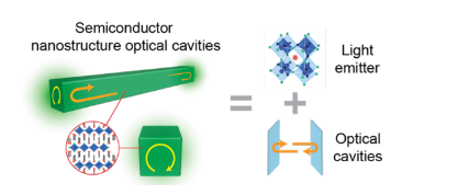
Figure demonstrating behavior of optical cavities within semiconductor nanowires. Credit: Kim Research Group.
While perovskite containing a three-dimensional lattice network has attracted plentiful attention for its optical and semiconductor qualities in nanowires, Kim is choosing to analyze layered two-dimensional perovskite, which has rarely been used in wire creation. Typically, in the bottom-up method of nanofabrication—singular atoms and molecules built up into nanostructures via chemical reaction—researchers utilize a solution-based approach. However, using such an approach for two-dimensional perovskite often results in a wide, thin sheet of material—not unlike graphene—rather than the desired nanowire structures. To tackle the issue, Kim is spearheading in his lab a process known as chemical vapor deposition (CVD). Here, nanofabrication is guided by constantly supplying gases and pulling vacuum through a highly automated system. The result is an approach to nanowire growth with a particularly high degree of control. “It’s very easy for us to investigate a range of conditions,” Kim says. “With wide ranges of both temperatures and pressures, we can systematically study the synthesis of these materials.”
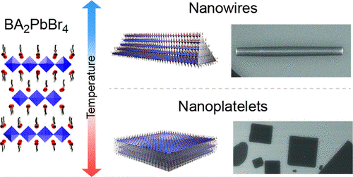
Synthesis of various perovskite nanostructures accomplished via CVD. Credit: Kim Research Group. Chem. Mater article, “Morphology-Controlled Vapor-Phase Nanowire Growth with Ruddlesden–Popper Lead Bromide Perovskite.”
The laboratory precision required to accurately analyze phenomena at the nanoscale means the Kim group must design and maintain its own custom instruments—a key component of Professor Kim’s outlook as a mentor and teacher, especially as a portion of the award will be used to fund a graduate student who will continue to develop their instrumentation knowledge: “My philosophy is similar to my own experiences in graduate school—it’s incredibly important for students to understand their equipment and work with it firsthand, never just ‘pressing the button and letting it go.’ So, in addition to knowledge of materials and photonic effects, a student will need to know how to build, modify, and troubleshoot their equipment—the nuts and bolts of vacuum fittings, flanges, and hole diameters.”
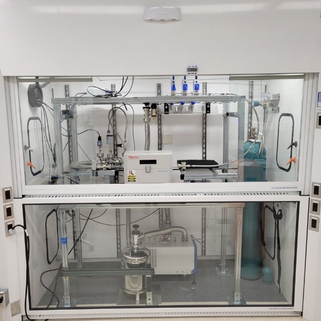
Chemical vapor deposition (CVD) instruments used in nanowire synthesis. Credit: Kim Research Group.
Looking ahead, the Kim group will build on its discoveries to fine-tune the creation of perovskite nanowires via CVD. “We have great crystal quality so far, but there’s room for improvement,” Kim offers. “For example, increasing quantum efficiency by changing oriented ligands or organic cations in the hybrid perovskite, resulting in different chemical structures—aromatic rings versus chains, or monoamines versus diamines. There’s so much microstructure that we can play with. These are the sort of next steps we’re taking.” Such work will benefit from research collaborators in Michigan State Chemistry and beyond, including Dr. Gary Blanchard (MSU), Dr. Elad Harel (MSU), and Dr. Kyoung Eun Kweon (Lawrence Livermore National Laboratory).