Seokhyoung Kim
Research
Semiconductor Nanomaterials for Electrons, Light, and Energy
(Research Description PDF)
The Kim group conducts research on semiconducting nanomaterials and meta-optical systems to advance next-generation technologies in energy conversion, light manipulation in solids, and quantum information processing. We combine precise chemical synthesis, innovative doping strategies, and cutting-edge optical design to create materials and structures with exceptional control over their electronic, optical, and magnetic properties.
New Materials Discovery
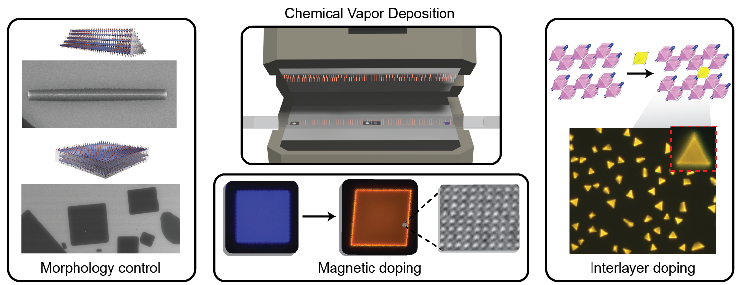
We design and grow novel nanomaterials using advanced chemical vapor deposition (CVD)
and wet-chemical synthesis, achieving precise control over lattice structure, morphology,
and composition. By tailoring dimensionality and crystal architecture, we uncover
new quantum and photonic behaviors and establish clear structure–property relationships
to enable high-performance device integration.
Unconventional Doping
We develop non-traditional, non-equilibrium doping methods that go beyond conventional
semiconductor design. By engineering charge-carrier behavior and light–matter interactions
at the nanoscale, we open pathways to transformative applications in optoelectronics,
spintronics, and spin-photonics.
Optical Metamaterials
We investigate meta-photonic phenomena in periodic nanostructures, focusing on 1D
dielectric “metawires” and nanowire superlattices capable of guiding, confining, and
manipulating light at subwavelength scales. Leveraging finite-element modeling, analytical
theory, and precision spectroscopy, we design optical bound states in the continuum
and high-Q resonances, enabling unprecedented spatial and spectral control for devices
such as tunable metasurfaces, solar cells, and quantum photonic circuits.
Contact / Webpage
Area(s) of Interest
Inorganic (In)
Material (Ma)
Physical (Ph)
Selected Publications
Mie-Resonant Three-Dimensional Metacrystals, S. Kim et al., Nano Letters, 2020, 20, 11, 8096–8101
Geometric Nanophotonics: Light Management in Single Nanowires through Morphology, S. Kim, J.F. Cahoon, Accounts of Chemical Research, 2019, 52, 12, 3511-3520
Photonics of Sub-Wavelength Nanowire Superlattices, S. Kim, MRS Advances, 2019, 4, 51-52, 2759-2769
Optical Bound States in the Continuum with Nanowire Geometric Superlattices, S. Kim, K.-H. Kim, J.F. Cahoon, Physical Review Letters, 2019, 122, 187402
Mie-Coupled Bound Guided States in Nanowire Geometric Superlattices, S. Kim et al., Nature Communications, 2018, 9, 2781
Self-Catalyzed Vapor-Liquid-Solid Growth of Lead Halide Nanowires and Conversion to Hybrid Perovskites, J.K. Meyers, S. Kim et al., Nano Letters, 2017, 17, 12, 7561–7568
Designing Morphology in Epitaxial Silicon Nanowires: The Role of Gold, Surface Chemistry, and Phosphorus Doping, S. Kim et al., ACS Nano, 2017, 11, 5, 4453–4462
CV
B.S., 2012 Pohang University of Science and Technology (POSTECH), South Korea
M.S., 2013 University of Massachusetts at Amherst
Ph.D., 2019 University of North Carolina at Chapel Hill
IIN Postdoctoral fellow, 2019-2020 Northwestern University
Assistant Professor, 2021-present Michigan State University
Awards
| Year | Award | Organization |
|---|---|---|
| 2019 | International Institute for Nanotechnology Postdoctoral Fellowship | IIN, Northwestern University |
| 2018 | Graduate Student Gold Award | Materials Research Society |
| 2014 | Kwanjeong Scholarship | Kwanjeong Educational Foundation |